By hFE of a Transistor 8294
What Is Transistor hFE: Basic Definition
Specifications and Key Characteristics of hFE
Importance of hFE in Circuit Design
Applications and Influencing Factors of hFE
How to Find a Transistor’s hFE
Practical Guide to Measuring and Adjusting hFE
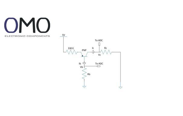
hFE is the DC current gain in the common emitter (CE) configuration of a transistor. It is the ratio of collector current (Ic) to base current (Ib):hFE = Ic / Ib
Symbol meaning:
Main function: hFE shows how well a transistor can use a small base current to control a larger collector current. It is a key indicator of amplification.
Application groups:
Ib > Ic(sat) / hFE(min)
This ensures the transistor is in deep saturation, where Vce(sat) is low. This reduces power loss.
Ib ≈ (2 to 10) × Ic(sat) / hFE(min)
Low hFE → low gain or wrong operation point.
High hFE → drift, saturation or cutoff distortion, or hard-to-turn-off issues in switching.
| Factor | Effect on hFE | Notes |
| Ic (Collector current) | Nonlinear | Low/high Ic → hFE drops. Mid-range Ic gives peak hFE. |
| Vce (Collector-Emitter voltage) | Negative | hFE drops when Vce is near saturation (<1V). |
| Junction temperature (Tj) | Positive | Silicon: higher Tj → higher hFE. Control temperature is important. |
| Device variation | Random spread | Same model/batch may vary ±20% or more. Use Min/Max for design. |
| Transistor type | Determining | Switch: low gain. Amplifier: high gain. Darlington: very high gain. |
| Frequency | Negative | hFE is DC value. For AC, use hfe (β) and fT (transition frequency). |
BC547A: 110–220
BC547B: 200–450
BC547C: 420–800
Transistor curve tracer:
This is the best tool. It shows the full output characteristic curves of Ic vs. Vce in real time. Each curve matches a constant base current (Ib). You can read the actual hFE at a specific working point (Vce', Ic') using:hFE' = Ic' / Ib'
Advantages: Clear and complete view. It covers all working areas (amplification, saturation, cutoff).
Disadvantages: Expensive and complex. Best for development stage.
Simple circuit setup (for learning the principle):
You can build this test circuit to understand how it works. Imagine the connection like this:
Vcc (+) → Rc (1-10kΩ) → Collector (C) → Transistor → Emitter (E) → GND.
Also, connect the base (B) to Vcc (+) through Rb (hundreds of kΩ to a few MΩ).
How to measure:
Set the working point:
Adjust Rb (or use a fixed Vb with emitter resistor Re) to make Vce close to the real working voltage.
Avoid the low-voltage saturation area!
Read and calculate:
Use the formula hFE = Ic / Ib.
What if results don’t match the datasheet?
Check these in order:
Negative feedback is the key:
Emitter resistor Re (local feedback):
When you add Re > 0Ω, the gain becomes:
Av ≈ -Rc / Re (if hFE * Re >> Rin).
In this case, gain is almost not related to hFE!
This is a common and effective way to make the gain stable.
Global feedback:
In a full amplifier system (like op-amps), use voltage or current negative feedback.
Darlington pair:
Use two transistors together. The total gain becomes:
hFE(eq) ≈ hFE1 * hFE2
This greatly reduces base current needs (Ic / (hFE1 * hFE2)).
It is good for switching circuits.
But it also increases Vce(sat) and switch delay.
Design margin for switching:
Ib = N * [Ic(sat) / hFE(min)],
where N = safety factor (usually 2 to 10, depending on how reliable it needs to be).
What to do:
Reduce base resistor Rb if needed.
Choose high-gain parts (if possible):
For amplifier designs, pick transistors with higher hFE(min) (e.g., use BC547C instead of BC547B).
This gives more gain margin.
In switching, higher hFE(min) allows larger Rb (less power used in driving) or makes it easier to reach deep saturation.
Direct calculation (from real values or design):
Use the basic formula:hFE = Ic / Ib
Step 1: Get the DC working point:
Make sure the transistor is in the right mode (amplifying or saturation).
Step 2: Accurate measurement:
Use ammeters in the circuit to measure Ic and Ib.
You can also use voltage drops across resistors to calculate the current.
Step 3: Simple division:
Just do Ic ÷ Ib to get hFE at that point.
Calculation from bias circuit (theoretical or reverse check):
What you need:
Know values like Vcc, base resistor Rb, and collector resistor Rc.
Basic example (fixed base bias, in active/amplifying mode):
Assume Vbe ≈ 0.7V for a silicon transistor:
Ib ≈ (Vcc − 0.7V) / Rb
In ideal active mode, Ic ≈ hFE * Ib,
but real Ic is limited by Rc and Vce:
Ic = (Vcc − Vce) / Rc
Combine the formulas:
hFE ≈ Ic / Ib ≈ [(Vcc − Vce) / Rc] ÷ [(Vcc − 0.7) / Rb]
≈ [(Vcc − Vce) * Rb] / [(Vcc − 0.7) * Rc]
Key difficulty:
This method needs you to know Vce, which depends on the load line and transistor properties.
You often need to measure Vce to get the real result.
Set your multimeter to its hFE or transistor testing function. Place the transistor in the dedicated socket, ensuring correct pin alignment. The hFE value will be displayed directly. Alternatively, in a fixed-bias circuit, measure the base current (Ib) and collector current (Ic), then calculate hFE using the ratio Ic/Ib.
hFE is the DC current gain parameter of a transistor, calculated as the ratio of collector current (Ic) to base current (Ib) (hFE = Ic/Ib) in steady-state operation. This parameter quantifies the transistor's amplification effectiveness, indicating how much larger the Ic is relative to the controlling Ib.
A transistor's hFE (DC current gain) governs its amplification of small base currents into large collector currents. This parameter directly influences the necessary biasing for stable operation. Higher hFE values enable stronger output signals with less base current drive.