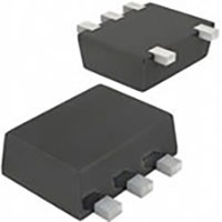
Toshiba has released two new load switch families, the ultra-low ON resistance TCK11xG and the low operating voltage TCK20xG. The new load switch ICs offer reverse current blocking and an over-thermal shutdown function. They can provide up to 2 A to 3 A of current, making them quite powerful for their small size.
The TCK111G and TCK112G feature ultra-low switch ON resistance, low quiescent current and a wide input voltage operation from 1.1 V to 5.5 V. Switch ON resistance is only 8.3 mΩ at 5.0 V and -1.5 A for load conditions. It also features an inrush current suppressing slew rate control driver and output auto-discharge function (offered as an option on the TCK112G). This is in a tiny chipscale package (1.0 mm x 1.5 mm, t: 0.5 mm) with 0.5 mm pitch.
The low-voltage load switches TCK206G, TCK207G, and TCK208G have smaller packages than the super-low RON family. They operate at voltages as low as 0.75 V, which makes them a good choice for being directly controlled by a low-voltage controller. They have an RON of approximately 18 mΩ, which is very low considering their even smaller chipscale package (0.9 mm x 0.9 mm, t: 0.5 mm) with 0.5 mm pitch.
For switches where voltage regulation is necessary, Toshiba provides low dropout (LDO) regulators. CMOS-LDO regulators have become the power management ICs of choice for mobile devices, as they enable a low profile, low supply current and low dropout. Toshiba's lineup of LDOs provides 200 mA to 300 mA of output current, with excellent noise-output and ripple rejection characteristics.
TCK111G and TCK112G Features
- Low ON resistance:
- RON = 8.3 mΩ (typ.) at VIN = 5.0 V, 1.5 A
- RON = 8.4 mΩ (typical) at VIN = 3.3 V, 1.5 A
- RON = 8.4 mΩ (typical) at VIN = 1.8 V, 1.5 A
- RON = 8.5 mΩ (typical) at VIN = 1.1 V, 1.5 A
- Wide input voltage operation: VIN = 1.1 V to 5.5 V
- Reverse current blocking
- Inrush current is limited by an internal slew rate control driver
- Thermal shutdown function
- Built-in auto-discharge (TCK112G)
- Pull-down connection between control and GND
- Ultra-small package: WCSP6C (1.0 mm x 1.5 mm, t: 0.5 mm (typical))
TCK111G and TCK112G Applications
- Power management
- Power delivery switch
- Active standby
- Low-quiescent power switch
- Mobile phones
- Tablet PCs
- Portable audio players
TCK206G, TCK207G, and TCK208G Features
- Low input voltage operation: V(IN)=0.75 V to 3.6 V
- Low ON resistance:
- RON = 18.1 mΩ (typical) at VIN = 3.3 V, 1.5 A
- RON = 18.2 mΩ (typical) at VIN = 1.2 V, 1.5 A
- RON = 18.4 mΩ (typical) at VIN = 0.75 V, 1.5 A
- Reverse current blocking
- Inrush current is limited by an internal slew rate control driver
- Thermal shutdown function
- Built-in auto-discharge (TCK207G and TCK208G)
- Ultra-small package: WCSP6C (1.0 mm x 1.5 mm, t: 0.5 mm (typical))
TCK206G, TCK207G, and TCK208G Applications
- Power management
- Power delivery switch
- Active standby
- Low-quiescent power switch
- Mobile phones
- Tablet PCs
- Portable audio players
Toshiba LDO lineup Features
- TCR2Exx low-noise LDO <200 mA
- TCR2DGxx performance LDO for minimal noise and ripple rejection <200 mA
- TCR3DMxx low-noise LDO <300 mA
- Variety of packaging from 0.8 mm x 0.8 mm 0.38 mm LGA to SOT-25
Toshiba LDO lineup Applications
- Power management
- Active standby
- Low quiescent
- Camera modules
- Low-noise sensors
- Mobile phones
- Tablet PCs
- Portable audio players