CDC2582

CDC2582
Mfr. #:
CDC2582
Fabricante:
Texas Instruments
Descripción:
Ciclo vital:
Nuevo de este fabricante.
Ficha de datos:
CDC2582 Ficha de datos
Entrega:
DHL FedEx Ups TNT EMS
Pago:
T/T Paypal Visa MoneyGram Western Union
ECAD Model:
Atributo del producto
Valor de atributo
Fabricante
Instrumentos Texas
categoria de producto
Reloj / temporización: generadores de reloj, PLL, sintetizadores de frecuencia
Serie
CDC2582
Escribe
Controlador de reloj PLL
embalaje
Embalaje alternativo de bandeja
Unidad de peso
0.009111 oz
Estilo de montaje
SMD / SMT
Paquete-Estuche
TQFP-52
Temperatura de funcionamiento
0°C ~ 70°C
Tipo de montaje
Montaje superficial
Suministro de voltaje
3 V ~ 3.6 V
Paquete de dispositivo de proveedor
52-TQFP (10x10)
PLL
Si con Bypass
Aporte
LVPECL
Producción
LVTTL
Número de circuitos
1
Relación de entrada: salida
1899/12/30 1:12:00
Entrada diferencial: Salida
Sí No
Frecuencia-Max
100MHz
Divisor-multiplicador
Sí Sí
Temperatura máxima de funcionamiento
+ 70 C
Temperatura mínima de funcionamiento
0 C
Suministro-Voltaje-Máx.
3.6 V
Suministro-Voltaje-Mín.
3 V
Tags
CDC2582, CDC258, CDC25, CDC2, CDC
Service Guarantees

We guarantee 100% customer satisfaction.

Quality Guarantees

We provide 90-360 days warranty.

If the items you received were not in perfect quality, we would be responsible for your refund or replacement, but the items must be returned in their original condition.
Our experienced sales team and tech support team back our services to satisfy all our customers.

we buy and manage excess electronic components, including excess inventory identified for disposal.
Email us if you have excess stock to sell.

Email: [email protected]
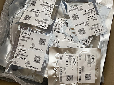
Step1: Vacuum Packaging with PL
Step1:
Vacuum Packaging with PL
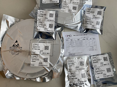
Step2: Anti-Static Bag
Step2:
Anti-Static Bag
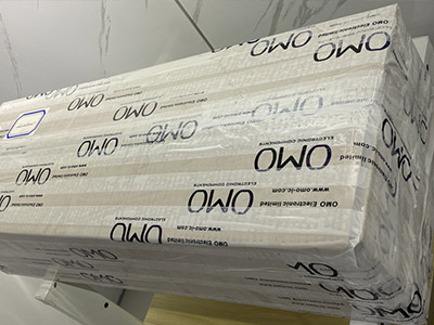
Step3: Packaging Boxes
Step3:
Packaging Boxes
***th Star Micro
the cdc2582 is a high-performance low-skew low-jitter clock driver. it uses a phase-lock loop (pll) to precisely align the frequency and phase of the clock output signals to the differential lvpecl clock (clkin ) input signals. it is specifically designed to operate at speeds from 50 mhz to 100 mhz or down to 25 mhz on outputs configured as half-frequency outputs. each output has an internal 26- series resistor that improves the signal integrity at the load. the cdc2582 operates at 3.3-v vcc. the feedback input (fbin) synchronizes the frequency of the output clocks with the input clock (clkin ) signals. one of the twelve output clocks must be fed back to fbin for the pll to maintain synchronization between the differential clkin and inputs and the outputs. view all in datasheet
***as Instruments
The CDC2582 is a high-performance, low-skew, low-jitter clock driver. It uses a phase-lock loop (PLL) to precisely align the frequency and phase of the clock output signals to the differential LVPECL clock (CLKIN, ) input signals. It is specifically designed to operate at speeds from 50 MHz to 100 MHz or down to 25 MHz on outputs configured as half-frequency outputs. Each output has an internal 26- series resistor that improves the signal integrity at the load. The CDC2582 operates at 3.3-V VCC. The feedback input (FBIN) synchronizes the frequency of the output clocks with the input clock (CLKIN, ) signals. One of the twelve output clocks must be fed back to FBIN for the PLL to maintain synchronization between the differential CLKIN and inputs and the outputs. The output used as feedback is synchronized to the same frequency as the clock (CLKIN and ) inputs. The Y outputs can be configured to switch in phase and at the same frequency as differential clock inputs (CLKIN and ). Select (SEL1, SEL0) inputs configure up to nine Y outputs, in banks of three, to operate at one-half or double the differential clock input frequency, depending upon the feedback configuration (see Tables 1 and 2). All output signal duty cycles are adjusted to 50% independent of the duty cycle at the input clocks. Output-enable () is provided for output control. When is high, the outputs are in the low state. When is low, the outputs are active. is negative-edge triggered and can be used to reset the outputs operating at half frequency. TEST is used for factory testing of the device and can be used to bypass the PLL. TEST should be strapped to GND for normal operation. Unlike many products containing a PLL, the CDC2582 does not require external RC networks. The loop filter for the PLL is included on chip, minimizing component count, board space, and cost. Because it is based on PLL circuitry, the CDC2582 requires a stabilization time to achieve phase lock of the feedback signal to the reference signal. This stabilization time is required following power up and application of a fixed-frequency, fixed-phase signal at CLKIN and , as well as following any changes to the PLL reference or feedback signal. Such changes occur upon change of SEL1 and SEL0, enabling the PLL via TEST, and upon enable of all outputs via . The CDC2582 is characterized for operation from 0°C to 70°C. detailed description of output configurations The voltage-controlled oscillator (VCO) used in the CDC2582 has a frequency range of 100 MHz to 200 MHz, twice the operating frequency range of the CDC2582 outputs. The output of the VCO is divided by 2 and by 4 to provide reference frequencies with a 50% duty cycle of one-half and one-fourth the VCO frequency. SEL0 and SEL1 determine which of the two signals are buffered to each bank of device outputs. One device output must be externally wired to FBIN to complete the PLL. The VCO operates such that the frequency of this output matches that of the CLKIN/ signals. In the case that a VCO/2 output is wired to FBIN, the VCO must operate at twice the CLKIN/frequency, resulting in device outputs that operate at the same or one-half the CLKIN/ frequency. If a VCO/4 output is wired to FBIN, the device outputs operate at the same or twice the CLKIN/frequency. output configuration A Output configuration A is valid when any output configured as a 1× frequency output in Table 1 is fed back to FBIN. The frequency range for the differential clock input is 50 MHz to 100 MHz when using output configuration A. Outputs configured as 1/2× outputs operate at half the input clock frequency, while outputs configured as 1× outputs operate at the same frequency as the differential clock input. NOTE: n = 1, 2, 3 output configuration B Output configuration B is valid when any output configured as a 1× frequency output in Table 2 is fed back to FBIN. The frequency range for the differential clock inputs is 25 MHz to 50 MHz when using output configuration B. Outputs configured as 1× outputs operate at the input clock frequency, while outputs configured as 2× outputs operate at double the frequency of the differential clock inputs. NOTE: n = 1, 2, 3
Parte # Mfg. Descripción Valores Precio
CDC2582PAH
DISTI # 296-6689-5-ND
Texas InstrumentsIC 3.3V PLL CLK-DRVR 52-TQFP
RoHS: Compliant
Min Qty: 160
Container: Tray
Limited Supply - Call
    CDC2582PAHG4
    DISTI # CDC2582PAHG4-ND
    Texas InstrumentsIC 3.3V PLL CLK-DRVR 52-TQFP
    RoHS: Compliant
    Min Qty: 160
    Container: Tray
    Limited Supply - Call
      CDC2582PAH
      DISTI # 595-CDC2582PAH
      Texas InstrumentsClock Drivers & Distribution 3.3V PLL Clock Drvr
      RoHS: Compliant
      0
        CDC2582PAHG4
        DISTI # 595-CDC2582PAHG4
        Texas InstrumentsClock Drivers & Distribution 3.3V PLL Clock Drvr
        RoHS: Compliant
        0
          CDC2582PAHTexas InstrumentsPLL Based Clock Driver, CDC Series, 12 True Output(s), 0 Inverted Output(s), BICMOS, PQFP52
          RoHS: Compliant
          15198
          • 1000:$7.9500
          • 500:$8.3700
          • 100:$8.7100
          • 25:$9.0800
          • 1:$9.7800
          CDC2582PAHTexas Instruments 1734
            CDC2582PAHTexas InstrumentsINSTOCK67
              Imagen Parte # Descripción
              CDCVF2509APW

              Mfr.#: CDCVF2509APW

              OMO.#: OMO-CDCVF2509APW

              Clock Drivers & Distribution 3.3V Ph-Lock Look Clock Driver
              CDCV855PWR

              Mfr.#: CDCV855PWR

              OMO.#: OMO-CDCV855PWR

              Clock Drivers & Distribution 1:4 DDR PLL CLOCK DRIVERS
              CDCV850IDGGG4

              Mfr.#: CDCV850IDGGG4

              OMO.#: OMO-CDCV850IDGGG4

              Clock Drivers & Distribution 2.5V Ph Lock Loop Diff Clock Driver
              CDC328DB

              Mfr.#: CDC328DB

              OMO.#: OMO-CDC328DB-1190

              - Bulk (Alt: CDC328DB)
              CDC421312RGER

              Mfr.#: CDC421312RGER

              OMO.#: OMO-CDC421312RGER-TEXAS-INSTRUMENTS

              IC CLK GENERATOR 312.50MHZ 24QFN
              CDCE906

              Mfr.#: CDCE906

              OMO.#: OMO-CDCE906-1190

              Nuevo y original
              CDCKV2310PWR

              Mfr.#: CDCKV2310PWR

              OMO.#: OMO-CDCKV2310PWR-1190

              Nuevo y original
              CDC2351QDBRG4

              Mfr.#: CDC2351QDBRG4

              OMO.#: OMO-CDC2351QDBRG4-TEXAS-INSTRUMENTS

              IC CLK BUFFER 1:10 100MHZ 24SSOP
              CDC337DWG4

              Mfr.#: CDC337DWG4

              OMO.#: OMO-CDC337DWG4-TEXAS-INSTRUMENTS

              IC CLK BUFFER 1:8 80MHZ 20SOIC
              CDC5D23BNP-5R6MC-CUT TAPE

              Mfr.#: CDC5D23BNP-5R6MC-CUT TAPE

              OMO.#: OMO-CDC5D23BNP-5R6MC-CUT-TAPE-1190

              Nuevo y original
              Disponibilidad
              Valores:
              Available
              En orden:
              1000
              Ingrese la cantidad:
              El precio actual de CDC2582 es solo de referencia, si desea obtener el mejor precio, envíe una consulta o envíe un correo electrónico directo a nuestro equipo de ventas [email protected]
              Precio de referencia (USD)
              Cantidad
              Precio unitario
              Ext. Precio
              1
              0,00 US$
              0,00 US$
              10
              0,00 US$
              0,00 US$
              100
              0,00 US$
              0,00 US$
              500
              0,00 US$
              0,00 US$
              1000
              0,00 US$
              0,00 US$
              Debido a la escasez de semiconductores a partir de 2021, el precio inferior es el precio normal antes de 2021. Envíe una consulta para confirmar.
              Empezar con
              Top