CD4056BNSRG4

CD4056BNSRG4
Mfr. #:
CD4056BNSRG4
Descripción:
IC BCD-7SEG DECODER/DVR 16SO
Ciclo vital:
Nuevo de este fabricante.
Ficha de datos:
CD4056BNSRG4 Ficha de datos
Entrega:
DHL FedEx Ups TNT EMS
Pago:
T/T Paypal Visa MoneyGram Western Union
ECAD Model:
Más información:
CD4056BNSRG4 más información CD4056BNSRG4 Product Details
Atributo del producto
Valor de atributo
Fabricante
Instrumentos Texas
categoria de producto
PMIC - Controladores de pantalla
Serie
-
embalaje
Tape & Reel (TR)
Paquete-Estuche
16-SOIC (0.209", 5.30mm Width)
Temperatura de funcionamiento
-55°C ~ 125°C
Tipo de montaje
Montaje superficial
Interfaz
BCD
Suministro de voltaje
3 V ~ 18 V
Paquete de dispositivo de proveedor
16-SO
Configuración
7 Segment
Suministro de corriente
0.04μA
Tipo de visualización
LCD
Dígitos o caracteres
1 Digit
Tags
CD4056BNSR, CD4056BN, CD4056, CD405, CD40, CD4
Service Guarantees

We guarantee 100% customer satisfaction.

Quality Guarantees

We provide 90-360 days warranty.

If the items you received were not in perfect quality, we would be responsible for your refund or replacement, but the items must be returned in their original condition.
Our experienced sales team and tech support team back our services to satisfy all our customers.

we buy and manage excess electronic components, including excess inventory identified for disposal.
Email us if you have excess stock to sell.

Email: [email protected]
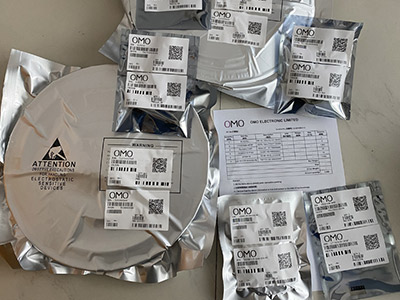
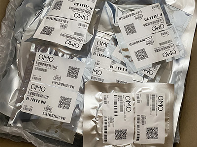
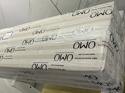
Step1: Vacuum Packaging with PL
Step1:
Vacuum Packaging with PL
Step2: Anti-Static Bag
Step2:
Anti-Static Bag
Step3: Packaging Boxes
Step3:
Packaging Boxes
***i-Key
IC BCD-7SEG DECODER/DVR 16SO
***as Instruments
CD4055B and CD4056B types are single-digit BCD-to-7-segment decoder/driver circuits that provide level-shifting functions on the chip. This feature permits the BCD input-signal swings (VDD to VSS) to be the same as or different from the 7-segment output-signal swings (VDD to VEE). For example, the BCD input-signal (VDD to VSS) may be as small as 0 to -3 V, whereas the output-display drive-signal swing (VDD to VEE) may be as large as from 0 to -15 V. If VDD to VEE exceeds 15 V, VDD to VSS should be at least 4V (0 to -4V). The 7-segment outputs are controlled by the DISPLAY-FREQUENCY (DF) input which causes the selected segment outputs to be low, high, or a square-wave output (for liquid-crystal displays). When the DF input is low the output segments will be high when selected by the BCD inputs. When the DF input is high, the output segments will be low when selected by the BCD inputs. When a square-wave is present at the DF input, the selected segments will have a square-wave output that is 180 out of phase with the DF input. Those segments which are not selected will have a square-wave output that is in phase with the input. DF square-wave repetition rates for liquid-crystal displays usually range form 30 Hz (well above flicker rate) to 200 Hz (well below the upper limit of the liquid-crystal frequency response). The CD4055B provides a level-shifted high-amplitude DF output which is required for driving the common electrode in liquid-crystal displays. The CD4056B provides a strobed-latch function at the BCD inputs. Decoding of all input combinations on the CD4055B and CD4056B provides displays of 0 to 9 as well as L, P, H, A, -, and a blank position. The CD4054B provides level shifting similar to the CD4055B and CD4056B independently strobed latches, and common DF control on 4 signal lines. The CD4054B is intended to provide drive-signal compatibility with the CD4055B and CD4056B 7-segment decoder types for the decimal point, colon, polarity, and similar display lines. A level-shifted high-amplitude DF output can be obtained from any CD4054B output line by connecting the corresponding input and strobe lines to a low and high level, respectively and applying a square wave to DFIN. The CD4054B may also be utilized for logic-level "up conversion" or "down conversion". For example, input-signal swings (VDD to VSS) for +5 to 0 V can be converted to output-signal swings (VDD to VEE) of +5 to -5 V. The level-shifted function on all three types permits the use of different input- and output-signal swings. The input swings from a low level of VSS to a high level of VDD while the output swings from a low level of VEE to the same high level of VDD. Thus, the input and output swings can be selected independently of each other over a 3-to 18 V range. VSS may be connected to VEE when no level-shift function is required. For the CD4054B and CD4056B, data are transferred from input to output by placing a high voltage level at the strobe input. A low voltage at the strobe input latches the data input and the corresponding output segments remain selected (or non-selected) while the strobe is low. Whenever the level-shifing function is required, the CD4055B can be used by itself to drive a liquid-crystal display (Fig.16 and Fig.20). The CD4056B, however, must be used together with a CD4054B to provide the common DF output (Fig.19). The capability of extending the voltage swing on the negative end (this voltage cannot be extended on the positive end) can be used to advantage in the setup of Fig.18. Fig.17 is common to all three types. The CD4054B-, CD4055B-, and CD4056B-series types are supplied in 16-lead dual-in-line plastic packages (E suffix), 16-lead small-outline packages (M, M96, MT and NSR suffixes), and 16-lead thin shrink small-outline packages (PW and PWR suffixes). The CD4054B- and CD4056B-series types also are supplied in 16-lead hermetic dual-in-line ceramic packages (F3A suffix).
Parte # Descripción Valores Precio
CD4056BNSRG4
DISTI # CD4056BNSRG4-ND
IC BCD-7SEG DECODER/DVR 16SO
RoHS: Compliant
Min Qty: 2000
Container: Tape & Reel (TR)
Limited Supply - Call
    CD4056BNSRG4
    DISTI # 595-CD4056BNSRG4
    LCD Drivers CMOS BCD-to-7-Seg LCD Dec/Driver
    RoHS: Compliant
    0
      Imagen Parte # Descripción
      CD4056BE

      Mfr.#: CD4056BE

      OMO.#: OMO-CD4056BE

      LCD Drivers BCD to 7 Segment
      CD4056BF

      Mfr.#: CD4056BF

      OMO.#: OMO-CD4056BF-1190

      - Bulk (Alt: CD4056BF)
      CD4056BF3A   CD4056BF

      Mfr.#: CD4056BF3A CD4056BF

      OMO.#: OMO-CD4056BF3A-CD4056BF-1190

      Nuevo y original
      CD4056BFXT

      Mfr.#: CD4056BFXT

      OMO.#: OMO-CD4056BFXT-1190

      Nuevo y original
      CD4056BNS

      Mfr.#: CD4056BNS

      OMO.#: OMO-CD4056BNS-1190

      IC BCD-7SEG DECODER/DVR 16SO
      CD4056BMG4

      Mfr.#: CD4056BMG4

      OMO.#: OMO-CD4056BMG4-TEXAS-INSTRUMENTS

      IC BCD-7SEG DECODER/DRIVR 16SOIC
      CD4056BMTE4

      Mfr.#: CD4056BMTE4

      OMO.#: OMO-CD4056BMTE4-1190

      LCD Drivers CMOS BCD-to-7-Seg LCD Dec/Drive
      CD4056BEG4

      Mfr.#: CD4056BEG4

      OMO.#: OMO-CD4056BEG4-TEXAS-INSTRUMENTS

      IC BCD-7SEG DECODER/DVR 16-DIP
      CD4056BM96

      Mfr.#: CD4056BM96

      OMO.#: OMO-CD4056BM96-TEXAS-INSTRUMENTS

      Nuevo y original
      CD4056BM

      Mfr.#: CD4056BM

      OMO.#: OMO-CD4056BM-TEXAS-INSTRUMENTS

      Nuevo y original
      Disponibilidad
      Valores:
      Available
      En orden:
      3000
      Ingrese la cantidad:
      El precio actual de CD4056BNSRG4 es solo de referencia, si desea obtener el mejor precio, envíe una consulta o envíe un correo electrónico directo a nuestro equipo de ventas [email protected]
      Precio de referencia (USD)
      Cantidad
      Precio unitario
      Ext. Precio
      1
      0,00 US$
      0,00 US$
      10
      0,00 US$
      0,00 US$
      100
      0,00 US$
      0,00 US$
      500
      0,00 US$
      0,00 US$
      1000
      0,00 US$
      0,00 US$
      Debido a la escasez de semiconductores a partir de 2021, el precio inferior es el precio normal antes de 2021. Envíe una consulta para confirmar.
      Empezar con
      Nuevos productos
      • CC2540 Bluetooth System-on-Chip
        OMO Electronic' CC2540 is a cost-effective, low-power, true system-on-chip (SoC) for Bluetooth® low energy applications.
      • Compare CD4056BNSRG4
        CD4056BNSR vs CD4056BNSRE4 vs CD4056BNSRG4
      • LP5907 Linear Regulator
        LP5907 linear regulators have low quiescent current and lead its class in noise performance without the use for a noise bypass capacitor.
      • CC2630/40/50 SimpleLink Wireless MCUs
        The OMO Electronic' CC2630 / CC2640 / CC2650 family of cost-effective, ultra-low power, 2.4 GHz RF devices have very-low active RF and MCU current.
      • MSP-TS430RGZ48C Target Board
        MSP-TS430RGZ48C target boards feature unified FRAM memory, enhanced MSP430 DNA, and integrated analog and digital peripherals.
      • TPA3144D2 Class-D Audio Power Amplifier
        OMO Electronic' TPA3144D2 is an efficient, Class-D audio power amplifier for driving bridged-tied stereo speakers at up to 6 W, 6 Ω, or 8 Ω (per channel).
      Top